Share the post "Samsung Electronics to Supply Ultra-Fast HBM2 on Full-Scale"
Samsung Electronics is planning to expand supply of ultra-fast HBM2 (High Bandwidth Memory), which is applied with Samsung Electronics’ 3D stacking technology and greatly improves bandwidth, on full-scale. This product will be used for high-performance AI (Artificial Intelligence) processor and network and GPU. Samsung Electronics announced that it is going to dominate this market by increasing its mass-production capability faster than its competitors.
Samsung Electronics announced on the 18th that it is planning to quickly increase supply of mass-production of 8GB HBM2 DRAM. 8GB HBM2 DRAM can receive and send 256GB of data per second which is 8 times faster than current graphic DRAM (8Gb, GDDR5, 8Gbps) that can send 32GB of data per second. This speed corresponds to a speed that can send 13 20GB movies with 4K resolution in just one second.

8GB HBM2 DRAM will be produced through TSV (Through Silicon Via) technology. TSV is a state-of-the-art stacking technology that drills very fine holes on chips, vertically stacks identical chips, and forms an electrode by filling holes with copper. 850 of major patents such as ultra-high integrated TSV design and heating control technology, which are developed by Samsung Electronics, are applied to this technology. Samsung Electronics also co-developed TC (Thermal Compression) bonding equipment that greatly increases efficiency while chips are being stacked by installing 8 heads. (Reference: 2nd page of The Electronic Times published on 5/31/17)
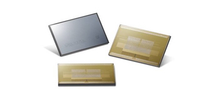
Actual picture of Samsung Electronics’ 8GB HBM2 DRAM (Provided by Samsung Electronics)
Samsung Electronics’ new product has 8GB HBM2 DRAM chips (based on 20-nano process) stacked on top of a buffer chip. Each chip is applied with ultra-high integrated TSV design that drills more than 5,000 fine holes on each chip and vertically stacks chips with more than 40,000 ‘TSV bumps’. Samsung Electronics has developed this new product so that it will maintain its optimum performance and not have reduced performance by switching a path to different TSV when transmission of data is delayed from certain TSV during processing of large amount of information. Samsung Electronics has also secured high level of credibility of its products by developing and applying its heating control technology that keeps particular areas of a chip under maximum temperature allowed during fast operations.
Also it is expected that this new product will contribute in overcoming limitations of AI system’s performance as it provides twice more of capacity than 4GB HBM2 DRAM while having a same size.
"By increasing supply of 8GB HBM2 DRAM, which is only mass-produced by Samsung Electronics, we are able to help our customers to release their next-generation systems on time." said Vice-President Han Jae-soo of Samsung Electronics Memory Business Department Strategy Marketing Team. "We are going to strengthen business partnership with variety of global customers by releasing lineup of next-generation HBM2 DRAMs."

After starting to mass-produce 8GB HBM2 DRAMs in June of last year and pioneering markets for supercomputer memories that are used for AI’s arithmetic operations, Samsung Electronics has expanded its business towards markets for current high-performance graphic card. Samsung Electronics is planning to be very active in responding towards demands from premium DRAM markets by expanding mass-production of 8GB HBM2 products according to requests from global IT customers in the future and increasing percentage of 8GB HBM2 products by more than 50% out of entire HBM products during first half of next year.
Staff Reporter Han, Juyeop | [email protected]
Share the post "Samsung Electronics to Supply Ultra-Fast HBM2 on Full-Scale"

